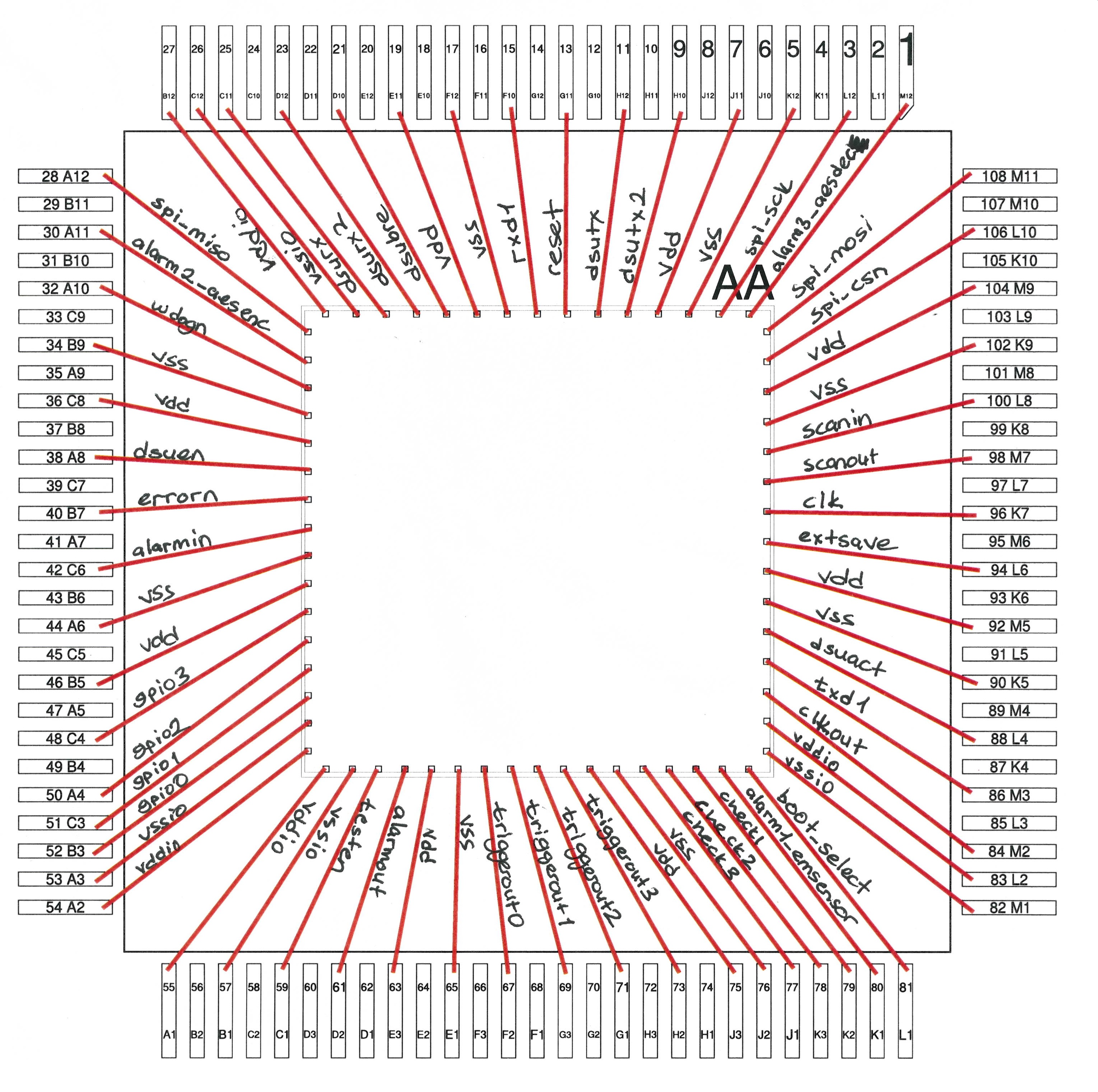
| alarm1_emsensor |
K1 |
Single pin Header output |
| alarm2_aesenc |
A11 |
Single pin Header output |
| alarm3_aesdec |
M12 |
Single pin Header output |
| alarmin |
C6 |
Jumper with GPIO0 to test TRAP HANDLER |
| alarmout |
D2 |
SMA |
| boot_select |
L1 |
VCC GND array on-chip/off-chip boot source select(0=on-chip, 1=offchip) |
| check1 |
K2 |
VCC GND array |
| check2 |
K3 |
VCC GND array |
| check3 |
J1 |
Single pin Header output |
| clk |
K7 |
Jumper select between on board, external(SMA) |
| clkout |
M2 |
SMA |
| dsuact |
L4 |
LED |
| dsubre |
D10 |
VCC GND array (DNP) need to be set to value of 0 |
| dsuen |
A8 |
VCC GND array (DNP) need to set to value of 1 |
| dsutx1 |
H12 |
PC |
| dsurx1 |
C11 |
PC |
| dsutx2 |
H10 |
|
| dsurx2 |
D12 |
|
| errorn |
B7 |
LED & MSP LED only |
| extsave |
L6 |
Jumper with Alarmout |
| gpio0 |
B3 |
Single pin Header output |
| gpio1 |
C3 |
Single pin Header output |
| gpio2 |
A4 |
Single pin Header output |
| gpio3 |
C4 |
Single pin Header output |
| reset |
G11 |
|
| txd1 |
M3 |
PC |
| rxd1 |
F10 |
PC |
| scanin |
L8 |
connect to pin Header |
| scanout |
M7 |
connect to pin Header |
| spi_csn |
L10 |
To Flash |
| spi_mosi |
M11 |
To Flash and external programming header |
| spi_sck |
L12 |
To Flash and external programming header |
| spio_miso |
A12 |
To Flash and external programming header |
| testen |
C1 |
VCC GND array (DNP) need to connect to GND |
| triggerout0 |
F2 |
SMA + Header |
| triggerout1 |
G3 |
SMA + Header |
| triggerout2 |
G1 |
SMA + Header |
| triggerout3 |
H2 |
SMA + Header |
| vdd |
E11, J11, M9, M5, J3, E3, B5, C8 |
|
| vddio |
B12, L2, A1, A2 |
|
| vss |
F12, K12, K9, K5, J2, E1, A6, B9 |
|
| vssio |
C12, M1, B1, A3 |
|
| wdogn |
A10 |
|